A Home Built (almost) Panasonic/MKE/CR56x CD-ROM Interface
I've got it to work.
Author :Gary Tait,VE3VBF
This project is based on info provided by Theo Markettos.
And by the C source code of a Linux driver by Zoltan Vorosbaranyi
Please don't bother me with programming info, or implementation of
a Panasonic CDR56x series drive as a stanalone CD player, as I don't
know any programming details. I suggest you peruse the Linux driver source code.
(source local mirror).
Here is a schematic for the main circuit.
Here is a schematic for the address decoder.
Here is a different schematic for the main circuit. (missing)
Here is different schematic for the address decoder. (missing)
All ICs are TTL 74LSxx types.
The project I am working on was a discrete component paralell printer
port adapter . The address decoder consists of a 74LS138, and a 74LS10,
and a 74ls367 (2+4 gated inverter).The original addresses were jumper selectable 0x278 and 0x378.
A3 is inverted, now producing 0x270 and 0x370 addresses. It has a 74LS32 to help
produce enable lines (by ORing an output of the '138 with either IOR
or IOW) ,a 74LS245 ,and had a 74LS367 (2+4 gated buffer)
The '367 and '368 each have 4 gates controlled by one address line,
and 2 gates controlled by another. (the chips have identical pinout,except
the 368 output is inverted).
I salvaged a shrouded 40 pin header from some old piece of equipment,
and attached it to the to edge of the adapter card.
Main Circuit:
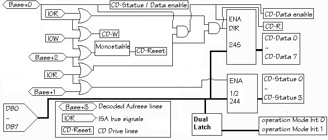
- CD-Data 0-7 - through 74LS245 octal Bus
Transciever to db0-7
245 Enabled when low on Base+0 AND [Base+2 OR IOR]
245 Dir- low when [Base+0 OR IOR] AND [Base+1 OR IOR]
- CD-Status 0-3 input through gated quad buffer (I use 1/2 74LS244) to
db0-3,
Enabled when low on when IOR OR Base+1
- CD-Reset IOW OR base+2
- Operation Mode bits 0-1 latched to db0-1 when low on IOW OR Base +3
The chip used is a 74LS175.
- CD-Status/Data Enable - Low when Base+0 (low when
status/info is read from or sent to drive,high otherwise)
- CD-Data enable - Connected to 245 enable
- CD-Read -Connected to 245 dir (low when reading info/status/data from drive)
- CD-Write low when I/O Write OR Base+0
Address decoder
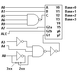
The 138 is enabled when G2A,and G2B are low ,and G1 is high.
G2A is controlled by A7 (x8x)
G2B is controlled by ALE
For 0x370,G1 is controlled by NOT [ NAND [NOT A3] ,A8,A4]. A8 is
inverted for 0x270.
C is controlled by NAND A5,A6,A9
B is controlled by A1
A is controlled by A0
Logic and Parts notes
The OR operations are each carried out by 1/4 of a 74LS32 Quad 2 input OR gate
The AND operations are each carried out by 1/4 of a 74LS08 Quad 2 input AND gate
The NOT operations are each carried out by 1/6 of a 74LS368 2+4 gatd invertor, with the gate lines
grounded, leaving a hex invertor.
The NAND Operations are each carried out by 1/3 of a 74LS10 Triple 3 input NAND gate
IOR is the I/O read signal (low when I/O read operation)
IOW is the I/O write signal (low when I/O write operation)
Base+x is decoded address line
CD-xxxxx is line on CD bus
Most signals are active low.
You can contact me at:taitg@hurontel.on.ca
Back to Theo's Panasonic CD page